Monday, 23 March 2020

Line Signal Muting

Line Signal Muting

While studying my Sony TC-K61 cassette deck, I was intrigued how the muting transistor action works? After sketching out a similar circuit of my own to analyse and assemble, I think I may now understand how this muting is achieved.

Here is Sony's muting circuit for the TC-K61 cassette deck for both recording and at Line Out - marked in green.


After sketching out my own generalised circuit, I had some components easy-to-hand, and so put this simple circuit together.
Here we have - an external signal generator shown to the left with its own internal resistance of around 600 ohms. Then I just added a simple, non-specific RC network to simulate general external circuitry. After that there is a load resistance of 20,000ohms. An oscilloscope was connected across the load RL.

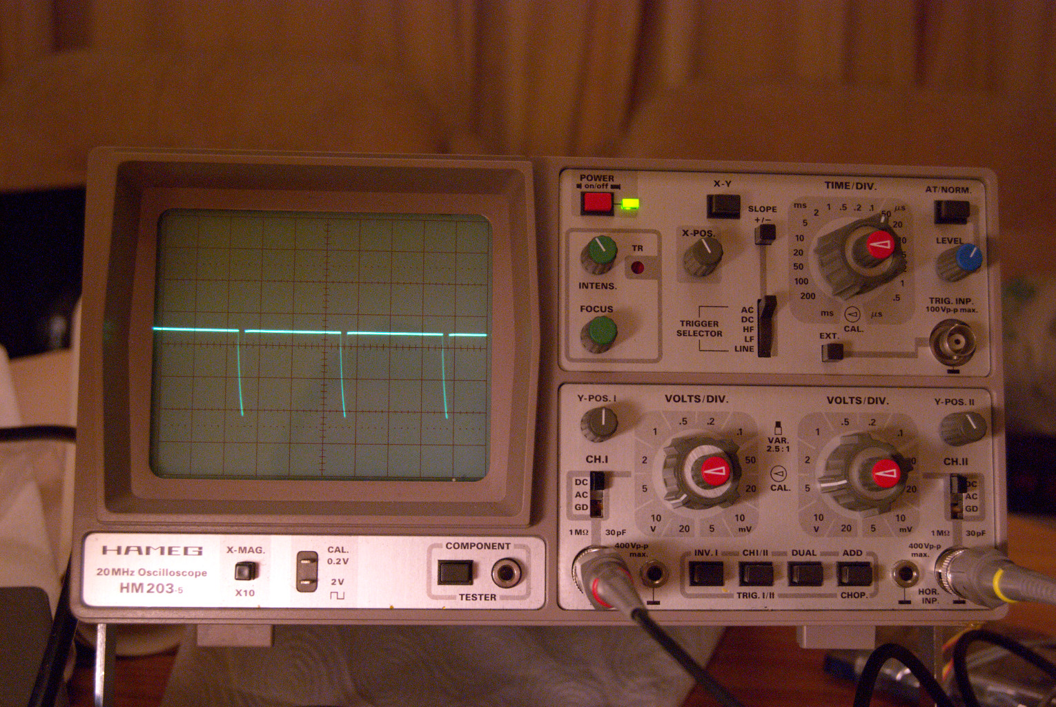
The muting transistor here is simply a S9014 NPN which is about to be switched 'on'. A sine wave signal voltage of 1Khz across RL was set to 2 volts peak-to-peak with no interference from the S9014. Once I had switch the S9014 'on', the output completely muted. 

The results ..

VL (before muting) = 2v.
VL (during muting) = 5mv.

This gave me an effective reduction of 20Log(0.005/2) or -52dB.

So why does this work?
Firstly, note that - the transmission line is effectively dc decoupled. Secondly, the S9014 is not experiencing any external one-directional electric field (hence voltage) to motivate charges across the collector-base-emitter junctions. 

So how does forward biasing the base-emitter junction result in an efficient -52dB muting reduction?

My theory: Both base-emitter, and base-collector junctions are forced into forward biasing modes.

There is no, or very little dc current running through RL, but since both forward biased junctions are now offering a conduction path, and in particular to an ac signal - it is this ac signal voltage component that gets shunted through both junctions as both junction slope resistances 𝚫V/
𝚫I (thanks to biasing) are very small.

Effectively, the source ac signal (component only) voltage drop, almost entirely occurs across the 600Ω, and 670
Ω+j/𝛚C impedances since the slope resistances (collector-base, base-emitter) are so low in comparison. It's basically potential divider law, the ac signal voltage at the two junctions is 'lost' earlier across the said impedances. *

(To understand slope resistance
𝚫V/𝚫I or slope conductance 𝚫I/𝚫V in this context, you'll need to study transistor NPN junction characteristics, and in particular the Ic vs Vbe (or even Ie vs Vbe) curve which are not always illustrated in datasheets) *
Shunting of the ac signal works in both directions, only one direction shown above.
Can we expect a forward biased base-emitter junction to offer a better conduction path than that of a forward biased base-collector junction?, probably, but I haven't investigated this.

I noted that during this electrical state, there was a very small dc potential across RL (collector-emitter) of 6.9mV, and again 6.9mV when I completely removed the circuit to the left of the S9014. This suggests that while one junction (probably base-emitter) was approximately 0.7v (forward biased), the other PN junction was at around 0.7v-0.0069v; effectively the same!

One final note - efficient muting was also realised when I reversed both emitter and collector.

23/03/2020.

2nd revision, 24/3/2020.
** 3rd revision: 20/03/2024
 

********************************************************************************
I also later simulated the circuit in https://www.falstad.com/circuit/circuitjs.html

The results were different concerning muting ability - this simulation was less efficient for some reason?, but the remaining analysis was reasonably accurate. You can see that both PN junctions were effectively forward biased and the slope resistance very low.


25/03/2020.

Wednesday, 18 March 2020

Recording/Playback Level Instability

Sony TC-K61 Recording/Playback Level Instability


For some time now, I have noticed that the deck's ability to record and playback at stable levels is questionable. Quite often I would have to recalibrate the playback levels (via 400Hz Dolby Level ref tape), and re-configure the record levels for my Maxell UR tapes. These random deviations from the target values were not small, but in the order of 2dB-4dB.

Frequently, it was the left channel that began to vary with time - was an hfe or hFE (ac and dc current gain) transistor parameter drifting as the deck warms up in the playback circuit? - if so, which one? Often small variations in hfe in a circuit with negative feedback have little effect. However, with reference to the playback circuit below - are the signal inverting transistors Q104/Q204 exhibiting problems?

New Components: So far I have replaced every capacitor in the audio and control boards, including all bias frequency generator capacitors. The bias frequency is stable at 100Khz, and generates around 30v (peak-to-peak) for Type I tapes at the record head terminals. Type II setting yields 34v, and about 65v for Type IV tapes.

Signal Path Relay: I even changed the Record/Replay Head signal relay to eliminate any possibility of a potentially and slowly oxidizing contact?

Old G2V-2 relay replaced with OMRON G5V-2. Note: old caps were still in circuit at the time of this image.

However, this full capacitor and relay replacement did not cure the problem, so what was it?

Playback Circuit: It was only recently that I began to study the playback circuit which consists of three transistors in an apparent Current Shunt negative feedback configuration - not Voltage Shunt as I originally thought? They are: 2SA836 (PNP), and the 2SC1345 (NPN). These are low power, low noise-figure (NF) transistors, which are no longer made.


There may be several schematic errors in the service manual?
Example: above Q103 and Q203 there are a biasing resistors in circuit, not capacitors.

2SC1345 Replacement: After searching the  internet for suitable replacements, I decided to 'chance' a KSC1845 Fairchild transistor which I had in stock. And which offered similar specifications - in particular dc hFE characteristics. As mentioned above, the basic purpose of Q104/Q204 is to act as a signal inverter, current-shunt negative feedback is later fed from Q105/205 to Q103/203.

From voltage measurements, the default 2SC1345 dc quiescent collector current for Q104/Q204 was approximately 310uA. Replacing both Left/Right channel 2SC1345 transistors with KSC1845s worked well - producing the precisely the same quiescent collector currents!!! Wow!


Board Modifications: Note - I have reversed the record and playback level potentiometers, re-soldering them so they are easily accessible. The 'new' KSC1845 NPN replacements are marked in red. (long pins)

Assessment: Currently, the replay amp is working well. After playback and record calibrations, the TC-K61 seems to have stabilized for both left and right channels.

Time will tell if I have found the source of the problem, fingers crossed!

Article subject to revisions, and correction of mistakes. 18/03/2020.
+10th minor revision, 31/03/2020.


26/03/2020: I have now replaced the Q103/203 and Q105/205 (2SA836 PNP) with Fairchild KSA922FBU PNP transistors, and recalibrated the TC-K61 - the deck's playback circuit is very stable! The dc quiescent collector currents Ic, and Vce quiescent voltages differed from the original 2SA836 configuration by between 2% to less than 5%. Virtually identical - good!

Finally, the buffer amplifier at the input line-in stage appears to be a simple emitter-follower configuration. The old (but not faulty) 2SC1345E was replaced with a Fairchild KSA1845FCK NPN transistor.


 The TC-K61 is working superbly well for Type I tapes!  

Thursday, 20 February 2020

Marantz SD35 Cassette Deck
Servicing and Alignment


Received this 1989 Marantz SD35 cassette deck off a relative - it had been in his loft for a number of years, and initially we didn't know if it was working. It was thankfully, and so now I thought it was time to check this thing out in more detail.
 
After the usual dusting or wiping off of debris, I opened the SD35 up and found that all was good internally. There was naturally some dust and corrosion present as expected, but was only minor.
 
I needed to investigate whether the drive belt needed replacing. The cassette tape transport and motor mechanism are cheaply made, and a bit delicate, so I had to handle with care. After extracting the mechanism from the main unit, I realised that to replace the belt meant more careful disassembly. I checked the elasticity of the drive belt, and everything seemed to be fine - so no need to fix that issue!
 

Cassette transport and motor - top right.

On reassembly, the machine worked but then a little later decided not to work!? The next day, I opened up the deck and carefully disassembled, and reassembled again the cassette transport unit. All was working back to normal!

Later, all external and internal potentiometers were switch-cleaned with Servisol, and then the heads and capstan were demagnetised.
 
Next on the to-do list was the record/replay head alignment - using an ABEX 10Khz reference tape I aligned the head azimuth to the tape. The original setting was out by a fair margin, ~ 180° at 10Khz.
 
So now I could use my ant-audio.co.uk 400Hz full track width Dolby Level reference tape to calibrate the output at Dolby Level, making sure both left and light channels were equal - I eventually settled for an output of slightly under 500mV (RMS) at Dolby Level.
 
At this point the peak reading LED meters were only a fraction out, but I re-calibrated these regardless. Unfortunately, in order to set the peak-level meters, I had to take the LED display and control board off the chassis and adjust in situ - thankfully it was not difficult.


I later calibrated the internal record levels to match that with the sensitivity of the current batch of Maxell UR C90 tapes. That is: record at 315/333/400Hz at 0VU or Dolby Level (Dolby Level = +2.7dB above 0VU), and the tape now plays back at calibrated level.


The deck is now playing well - very stable sound, very pleased.

Back in 1989, this retailed for around £149.99 in the UK.


Article subject to alterations and corrections without notice. 21/02/2020

Monday, 10 February 2020

Sansui SC-1330
Cassette Deck
Maintenance/Servicing


Bought off ebay for little money, this was advertised as ´For Spares or Repair´. It was in good physical condition, and the heads had very little wear. The pinch roller looked aged, but after some cleaning with isopropyl alcohol, and later filtered water on a cotton bud, it is nearly as good as new!

So far I have replaced the old drive belt - a 72mm or less diameter is fine, 3.5mm width, although I have just ordered a 64mm diameter 6mm width belt, let us see how that works later when it arrives!?  

12/2/2020: The 64mm diameter, 0.7mm thickness, and 6mm wide belt was more difficult to fit. Overall, the tension was too high, due mainly to the thickness (0.7mm) of the belt. Also, this belt wouldn't always run well - not sure why!? So I reverted back to the 72mm belt.

I think a 68mm-70mm diameter, 3.5mm-5mm width belt would be optimal?

Replaced most electrolytic capacitors, and cleaned all potentiometers with Servisol. 

Rubber Renew
Bought 125ml of this toxic chemical, and so decided to use on my machines. It smells like rubber solution, only stronger! I decided to buy this stuff hoping that it would return the power and hence internal 'grip' for the tape rewind, fast forward, and the take-up spool during recording. It did the job, but I had already cleaned much of the idler gears with isopropyl alcohol, and diluted acetone anyway - I'm not sure if Rubber Renew is worth the money?

If you use Rubber Renew, be sure to follow the safety instructions.

Noisy ON/OFF switch 
The Sansui SC-1330 makes a small electrical arc when switching on or off. This interference can be clearly heard through both headphones and the loudspeakers. On investigate I saw that the internal mains switch does not have any form of arcing/noise suppression.

After studying the circuit, I decided to bridge the switching contacts with high voltage rating, ceramic capacitors - marked below in blue.


The diagram above was taken from the service manual. I also noted that only Japanese versions of the SC-1300 series had suppression support!?

I carefully soldered in some 3Kv (not 3.3Kv as suggested in diagram) rated capacitors - yes these are probably over-rated, but best to be safe than sorry?! These completely eliminated any sound blips due to on-off switch arcing issues. I didn't bother to add a small resistance in series with the capacitors - these limit the transient currents which only last for some micro-seconds anyway. This type of suppression circuit is know as an RC Snubber Circuit.

My alteration to the mains board is shown below.


Sansui SC-1330 Calibration
I have also calibrated the machine so that -
  • Test Tape Input: 400Hz Dolby Level RefTape, gives Vout = 500mV (RMS)  or ∼1400mV p2p.
  • Calibrated the peak level meters to read Dolby Level at RefTape Dolby Level input.
  • Calibrated the internal Record Levels (for Maxell UR), this means .. record at 0VU, and achieve 0VU on playback etc.
  • Bias adjustment: 1000Hz to 10,000Hz flat for Maxell UR tape. 
  • Rec/Replay Head azimuth check with my ABEX 10Khz ref tape - the original setting was spot on!!!


21/02/2020

29/04/2020: I decided to give the shorter and stronger 64mm x 6mm belt another go. This time I had cleaned the pully wheel carefully, "roughing up" the surface for a better grip. I also allowed the flywheel to guide the line of the belt around the pulley - this was done by losening the pulley screws and turning the flywheel with my finger so that the belt would find a natural line, the pulley would then slide outward a little more. Finished this alignment by tightening the pulley grub screws.

Results: Both fast-forward (FF), and rewind (RW) are much better than before - no stalling!

So far, so good!
 

Friday, 6 December 2019

NAIM NAC32.5 and NAIM NAP110 Servicing.

This intended 'servicing' of the above old NAIM products, is going to be in 'slow motion', in other words - a slow, but on going job, and one that will reveal some discoveries, and pending problems - no doubt!

Not used '32.5' and the '110' for several years, I decided to fix a broken stereo/mono toggle switch, which from start to finish took nearly three hours.

In order to get the board out, I decided to desolder the rear DIN and phono connections. The replacement mini toggle switch was a Dual-Throw, Double-Pole type 'DTDP' with no 'latch' effect.


Top Toggle Swich was broken - no easy direct replacement available.

Having got the NAC 32.5 working again, I was puzzled that the pre-amp in mute mode didn't null-out the sound completely - something that I'd not noticed before? 

Working the NAP110 again
Switching on the NAP110 Power Amp soon revealed that something wasn't right - the NAC32.5 was not receiving 24v from the NAP110. The only indication that some power was getting through was a faint light from the LED on the 32.5. Re-connecting the NAP110, the NAC32.5, and a SNAPS unit (to run the 32.5) lead me to believe that the power supply from within the NAP110 was faulty? Both pre-amp (32.5) and amp (110) played well once the SNAPS unit was in use - although on occasion, a sort of disconnecting noise could be hear randomly. Further investigation later revealed that the regulators were not functioning properly.

A quick look into the NAP110 revealed that the amplifier's in built low-current LM317 voltage regulator (and/or 3300uF cap?) was faulty - only showing +2.9v dc, as opposed to +24v dc. This commonly used regulator circuit appears to supply any associated NAC controller of that era - I'm thinking mainly of the NAC 42, and NAC 32/32..5 series? 

Obviously, a few or all of the components need to be replaced, then some re-testing......


NAIM NAP 110 Power Amp with regulator for external provision.

With LM317 based regulator removed.

NAIM 36v-to-24v Voltage Regulator
 
The standard NAIM regulator for 36v-to-24v conversion is a common circuit configuration, but with additional ripple effect reduction via C2. 
 
This is able to reduce ripple to around -80dB, according to Art of Electronics (Paul Horowitz/Winfield Hill). Their research suggests a 1v ripple reduced to a mere 0.1mV!, at 60/120Hz I assume?

Below, I've drawn out the circuit.


The Components of the LM317 Design

Flywheel BYF406 diode: 1.0A Iout, 800V Vrrm, Fast Recovery Rectifier Diode. Operational temperature range from 0°C to 175°C. If a replacement is required I'll use a 1N4006 diode, although I only have the 1N4004 (1.0A Iout, 400v Vrrm) in stock, so maybe I'll use this instead? 

BYF406 Purpose: probably to shunt any charge from C2 should either C3 or the load 'short'. And additionally to protect the LM317T from any back emf if the load become immediately disconnected.

Capacitors: both 10uF capacitors are tantalum (a transition metal) bead types.

Resistors: Are all 5% tolerances.

Regulated Voltage Output: The Formula for output voltage Vo of the regulator is: Vo=1.25(1+R2/R1). And here (without error tolerances taken into consideration) we obtain..

Vo=1.25(1+3980/220) = 23.86volts.

So I can conclude that the layout 'checks out' nicely with the theory, and with parts currently in the post, I can look forward to rebuilding the regulator.

NAIM SNAPS for the NAP 110 System

Coincidentally, the NAIM SNAPS (power supply) unit also employs the same LM317 based regulator circuit, but here there are two of them.

To my complete disbelief, one of the regulators in this unit was also faulty, delivering zero output, that is 0V! While the other was working nicely at 23.7v dc. 
 
Seems, that this unit also requires a complete service too. I did note that the unit soon got warm after switch-on, an indication that the LM317 was shorting via C3?

11/12/2019: With reference to the NAP110 Power Amplifier
Replaced unit with new regulator: the LM317T, 2 x 10uF tantalum capacitors (where one had initially 'shorted'), and the flywheel/protection diode was replaced with 1N4004 type. 

Since then, I have been testing the NAP110 with my NAC32.5 - so far all working well!

The meter was flickering between 23.8v and 23.9v. The calculation above was 23.86v, the target is 24v.
Testing the NAC32.5 and NAP110 after regulator circuit fix.
12/12/2019: NAIM SNAPS unit now has had all LM317T and output 10uF 35v tantalum capacitors replaced in the voltage regulator circuit. Unit working well.

Large 10,000uF Electrolytics:

(18/12/2019) I will eventually replace all 10,000uF electrolytic capacitors in time - have just ordered KEMET 10,000uF 63V soldered-tag type (35mmx55mm). This is an over-specification, but I prefer to over-engineer. The original voltage limit of the old capacitors was 40volts. 

So far all units are working well!

Power-on Diode: (13/12/2019) The NAP110 power-on diode failed a long time ago, so I decided to replace it. Not sure of the exact specifications so I decided to put my own circuit in place - a simple red LED, in series with (effectively) 30K ohms. The supplied voltage to the circuit is approx 36v. I wanted to try to match the brightness of this with the brightness of my NAC 32.5 contoller's LED. After a few investigations, even 30K (10K+20K) ohms was not high enough resistance to create a good match, but it's good enough for now - I'll change it again later to perhaps 51K ohms?


The circuit is shown exposed (ie un-isolated) for the purpose of the photograph. I used an old small circuit board and adapted it, but I will re-configure it again with some veroboard I recently bought.

27/12/2019: Finally settled for 2 x 100K ohm in-series resistors for the LED, which gives a good match to that of the NAC 32.5 and SNAPS LED intensity - not quite the same, but close enough.
(The circuit has been modified slightly since I took this photograph)


The revised circuit board is isolated underneath with a rubber mat, cut from an old bicycle inner tube, super-glued and shaped to fit. The LED is temporarily centred with Blu Tack. There's no danger of the assembly falling out - with or without the Blu Tack. The hole in the fascia, is actually threaded, I didn't realise this until re-assembly.

Later on, I'll re-cap the NAP 110, and the SNAPS with new 10,000uF KEMET capacitors. These arrived this morning...


Also of note - a heavier duty full-wave diode rectifier for the power amp, which I may or may not fit later?

20/12/2019: The SNAPS unit is now fitted with a 10,000uF 63v KEMET electrolytic capacitor. The 'spades' on these are not as easy to work with as the original ITT capacitors. I applied plenty of solder and secured the initial soldered connection, and later went further by wrapping the soldered joints with wire, then applying more solder so that the original joint could never seperate. The downside of this additional procedure is that the joint 'looks' untidy from the outside - this I find a little annoying if I am honest!


(The servicing of the NAP 110, NAC 32.5, and SNAPS unit is unfinished. All working fine so far. 18/12/2019)
 

Wednesday, 6 November 2019

YAESU FRG 7700
Servicing, Discovery, & Issues


Basic Serving Objective
My initial task, was to service the receiver, and the first job was to replace all electrolytic capacitors on the top board. This was eventually achieved with no issues. As a matter of course, I also cleaned the post-soldering areas with isopropyl alcohol and an old tooth brush – its vital that no unintentional connections are made.

However, after replacing the KF2510 connectors I made a casual error – mistaking P17 for P24! The set worked initially for a short while, then one of the 10 ohm resistors began to heat up, something was obviously wrong! After studying the circuit and the circuit diagram, I replaced R248 (10 ohm ½ watt), and as a precaution both Q59 (C1384R NPN transistor), and D46 (10v zener diode). The set now worked fine.

FIP5A8B Display
The display is continuously updated from a single 7-segment (plus 1dp), 8-bit multiplexed data bus, were each digit value is allocated a quota of time. The 8-bit data is bused to the FIP5A8B unit from the MSM5524R microcontroller. Each digit within the FIP5A8B appears to be strobed or activated sequentially by Q52 to Q56 which are controlled by the MSM5524R.

Overall, the display works well, but I noted some years after I bought the FRG-7700 in 1981, that when in ‘DIM’ lit mode, all the display digits tended to leave the ‘c’ segment on the 7-segment display partially lit? This ‘c’ segment is the single segment which is vertical, on the bottom right. 


I originally suspected, and still do, that the MSM5524R Microcontroller has a minor fault somewhere within the workings of pin 29?, which is the 'c' segment in the a,b,c,e,d,e,f segment naming convention. 

It is as if the output transistor stage is not effectively switching fully in the OFF state? Oscilloscope traces indicate residual noise, which is possibly and effectively leaving this partially ON?


Only recently did I learn that in ‘DIM’ mode, pins 25-31 (7-segment data), and 35 (decimal point) have their pulse-widths narrowed when busing the data from the MSM5524R to the FIP5A8B - the oscilloscope traces confirm this.

Voltages and traces for all 7-segment pins (inc 29) when ..
logic state = Segment ON.
No DIM mode.
Pulse at full width.
Centre line = 0V (Earth)
Voltages and traces for all 7-segment pins (not inc 29) when ..
logic state = Segment ON.
DIM mode.
Pulse at reduced width.
Centre line = 0V (Earth)

At the partially faulty Pin 29 'c' segment.
logic state = Segment ON
DIM mode 
Plus at reduced width, plus noise 'blip'.
Note also: reduced negative potential.
Centre line = 0V (Earth)
Voltages and traces for all 7-segment pins (not 29) when ..
logic state = Segment OFF.
No DIM mode.
Centre line = 0V (Earth)
Pin 29 
logic state = Segment OFF
(Full Brightness or DIM mode, the traces are almost identical)
(Note: lessened negative voltage and noise)
Centre line = 0V (Earth)
It is apparent that all 7-segment data pins behave well - when any segment is ON, or OFF (full brightness or in DIM mode), but pin 29 (the 'c' segment) does not - clearly problems within the MSM5524R!?

So far, and to eliminate other possible causes (although unlikely) and for the sake of completeness I replaced all 7-segment display-digit synchronising transistors Q52 to Q56, plus all small rectifying and signal diodes (1SS53) all involving working the Astable Mulivibrator (a DC-DC Convertor). They are the D47..D50, D51,D52, D55, D56, D42, and D43 replaced with a common, but reliable 1N4148 type. Both Q60 and Q61 switching transistors in the Astable Multivibrator circuit were also replaced.  

Relative Potential at input of FIP5A8B
Negative DC potentials (wrt Earth) are highlighted below, and later the oscilloscope traces at the 7-segment data bus input to the FIP5A8B.

User's Manual states the rectified DC-DC Converter should produce -25v supply, but it is producing approximately -35v.

Digit Strobe/Sync Signals to FIP5A8B
Shown below are just two (of the five traces) at the bases of transistors: Q52, and Q53 as they consecutively switch ON and OFF the respective digits on the FIP5A8B display. Unfortunately, I don't have the facility to display all 5 at the same time.
'Low' state at 0V switches ON these Q52/Q53 PNP transistors.
Note the switching frequency: Approximately a 3ms period in the 5-digit update cycle. The whole 5 digit display appears to be updated (repeated) in 3ms or at about 333Hz.

FIP5A8B Clock Generation
The Astable Mulitvibrator and buffer transformer (form a DC-DC Convertor) appear to be the FRG-7700's generator for the FIP5A8B display 'clock'. The voltage trace shown is effectively across the input of the FIP5A8B, it's only approximately 4 volts peak-to-peak.

The clock frequency is calculated from f=1/T, 
where T is the period of the waveform. 

Since T=150us, therefore f=6667Hz.


Compare: FIP5A8B clock (6667Khz) to
MSM5524R (333Hz) 5-digit-block strobe frequency.
20:1 ratio.

Pull-up Resistor Bank
I also lifted the old resistor bank RB01 (8x 100K ohm) and replaced this with my own resistor network. 


All new components are marked on the circuit diagram below.

Note: Pin 29 'c' segment,which didn't switch cleanly from +5v to - 34v.

Front Dial Display Lamp
Later, the front dial display lamp (PL4001, 12v 100mA?) was replaced with a ‘white’ 5mm LED, in series with 2 x 220 ohm 1/8 watt resistors – the DC source was measured at approximately 10.6 volts.

Calculation is relatively easy: The full brightness of the LED is quoted at about 20mA. Without drawing the circuit diagram, and writing out Kirchoff's Voltage Law, the maths does arrive at ... (10.6 - 3)v/(2*220 ohms), which is approx 17mA. Not 'full on' brightness, but bright enough, the diode should last longer too!

White LED glued into a washer.
White 3v LED, glued washer 'gromit' and glued into place. 

I later isolated the LED and contacts from any possible electrical shorting.  

Zener Diodes at Display Driver Stages
Not stopping with this servicing adventure, I decided to change the two zener diodes D53 (7.5v), and the D45 (5.6v). The D45 is involved in fixing the voltage to about 5.6v and allowing the MSM5524R to apply 5v and activate the sync transistors for the FIP5A8B display unit. 

However, to my shock after switch on, the display only indicated one digit, which was random every time I switched on. I knew immediately what was happening – the synchronising transistors were not able to update any synch pulses to the digit display - they were locked out by some biasing error? To my disbelief, almost all of the pack of ten ‘5.6v’ zener diodes I bought were faulty! I quickly resolved the issue (for now) by returning the original 5.6v zener to its place.

Weakened Solder Joints
Through repetitive, but careful disassembly and assembly, the pins that hold the KF2510 connectors began to fracture the solder under-board, but not lifting the tracks. So as a precaution , I flowed fresh solder around the joints and their strength returned.

Ideas for the Front End Tuner Section
I may at some point, replace the signal diodes 1SS53 with BAT42 Schottky diodes, which have a lower forward voltage – somewhere around 250-350mV.  Will these allow the set to become more sensitive, especially at 21Mhz and higher?

Front End Signal Diodes Replaced (30/11/2019)
Just for experimental reasons, I de-soldered the old 1SS53 signal diodes, and carefully soldered in, a new set of BAT42 Schottky signal diodes. The BAT42s have a lower forward voltage. My thinking was - a more sensitive Front End? Results so far are very positive!


3/12/2019: Just replaced the two zener diodes that serve the display: D45 (5.6v), and D53 (7.5v). I've used 1watt zener diodes for no ther reason than to make sure that neither break down.

Latest shot of the top board, FIP5A8B display side.

Currently, the FRG 7700M is working very well! 
The article may still be subject to corrections without notice. Latest amendment: 3/12/2019.