Saturday, 28 October 2023

AKAI AT-2400 Stereo Tuner

 AKAI AT-2400 Stereo Tuner


I could not resist this on ebay - an AKAI AT-2400 Stereo Tuner which obviously needed some attention. It was reasonably priced and in a condition which I believed I could turn around.


The marks you see on the fascia are apparently nicotine stains. I certainly took some time to examine all the photographs in the advert for any signs that the tuner had been abused. Apart from the nicotine stains, there are other marks, the most prominent is to the bottom right corner where the brushed aluminum has been subject to some form of impact.

I decided to buy the tuner and on arrival I determined  if the tuner was 'basically' working, which it was. The next task was to disassembled the tuner, and in particular attempt to remove the nicotine from the front.

Servicing Work Undertaken

  1. Cleaned fascia, all control knobs and buttons. 
  2. Switch-cleaned all contacts and potentiometers, including calibration potentiometers.
  3. Replaced all electrolytic capacitors.
  4. Calibrated FM and AM where possible without the use of an oscilloscope (≥150Mhz bandwidth required) and RF signal generator.
  5. Adjusted the 'High Blend' mixing control to reduced the perception of stereo white/pink noise for weaker, or noisy stereo FM signals. 
  6. Replaced all Power Supply Unit (PSU) high voltage rated protection-capacitors for the rectifying diodes.
  7. Replaced PSU rectifying diodes.
  8. Replaced the 13v zener diode in the PSU.


Pending Work: Replace the PSU voltage regulation main transistor.

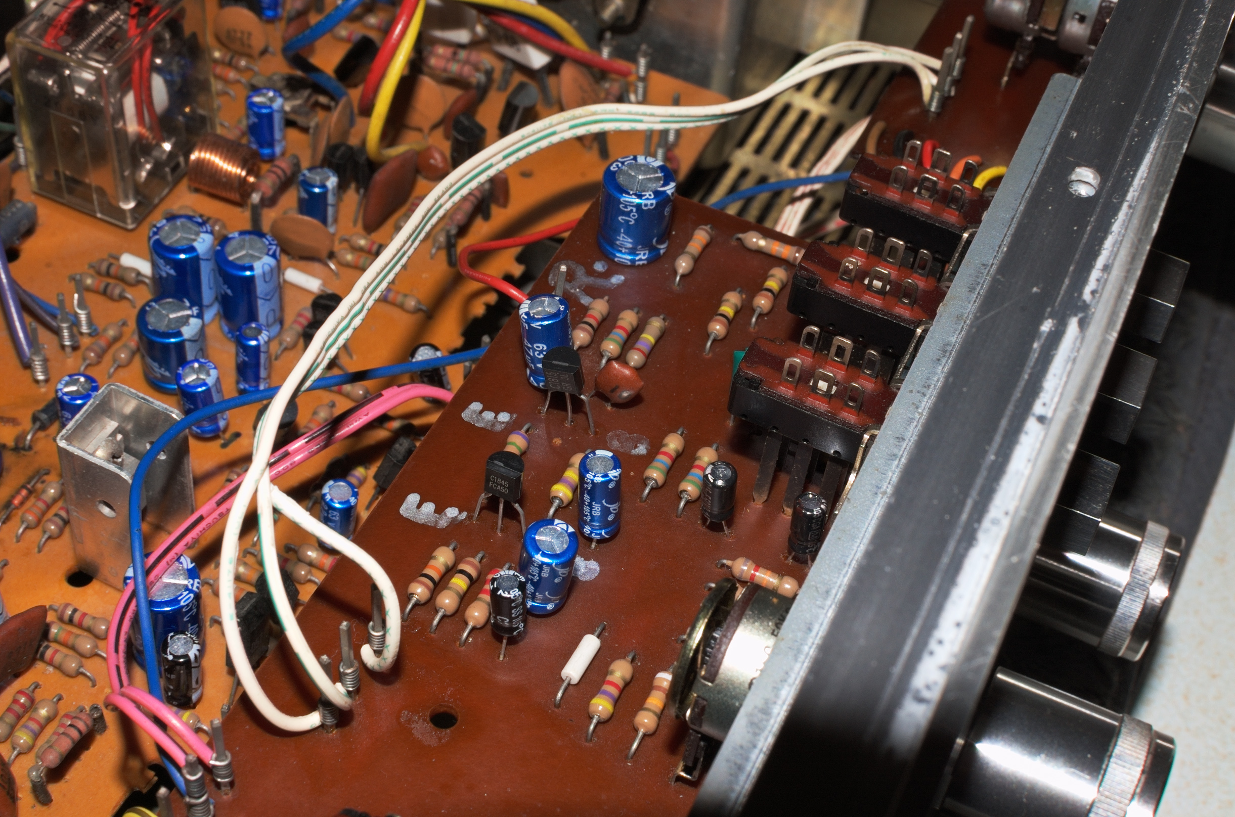
Shown below is a temporary replacement bridge rectifier and new high voltage diode-protection capacitors that protect the rectifying diodes - mainly during switch-on. At switch-on, there is often a high current surge or spike where the diodes are subjected to a high rate of change of voltage (high dv/dt) and thus high current. At all times, capacitors exhibit the electrical characteristic of i=CแงdV/dt amperes, and so these will help to bi-pass excessive transient current surge or spike.


After completing the first 9 tasks, the tuner is working fine, and looking good.

View From the Outside

The AKAI AT-2400 sits below the Trio KA-6100.

Adjusting High Blend Stereo Mixing

What is 'High Blend' as defined by AKAI?

From what I can glean from the the service manual, it appears that 'High Blend' is a technique to reduce background high frequency low level interference, or white/pink noise when reception conditions are not favourable.

To achieve this, the stereo image is narrowed with much greater emphasis placed on higher audio frequencies. Background noise is far more noticeable if the noise is stereophonic, rather than monophonic. Monophonic noise is 'in phase', in contrast - stereophonic is not.

The method AKAI employed was to mix left and right channels, but only with increasing audio frequency.

Observing the diagram below partially illustrates how they did this.


The Sanyo LA3122 IC is a dual channel high gain voltage amplifier, similar to a modern OP Amp today. The Voltage-Series negative feedback network loop from pin 5 (or 10) to pin 3 (or 12) dictates gain and applied filtering characteristics if needed.

To the left of this circuit, is the 'High Blend' mixing unit - a simple but effective capacitor circuit of just 15nF is placed across both left and right channel inputs. Since capacitive reactance is given by 1/{2๐›‘fC} โ„ฆ, increasing either capacitance C, or frequency f will lower the reactance (ie, lower impedance), and so at higher capacitance or higher frequencies the audio is mixed and placed towards the centre of the stereo image.

To make this more effective, the original C14 was swapped for a 22nF polyester capacitor. I may even try 27nF at a later date?

Sanyo LA3155 and LA3122

Sanyo's LA3122 and LA3155 high gain voltage amplifiers have been used for potentially many applications including: audio phono (moving magnet) cartridge amplification with RIAA playback de-emphasis, IEC/NAB de-emphasis for tape recorder playback, an active low pass or high pass filter, and of course as a simple voltage amplifier with constant gain.

The LA3155/3122 series is centered around a three stage NPN voltage amplifier with an open loop gain of several thousand.


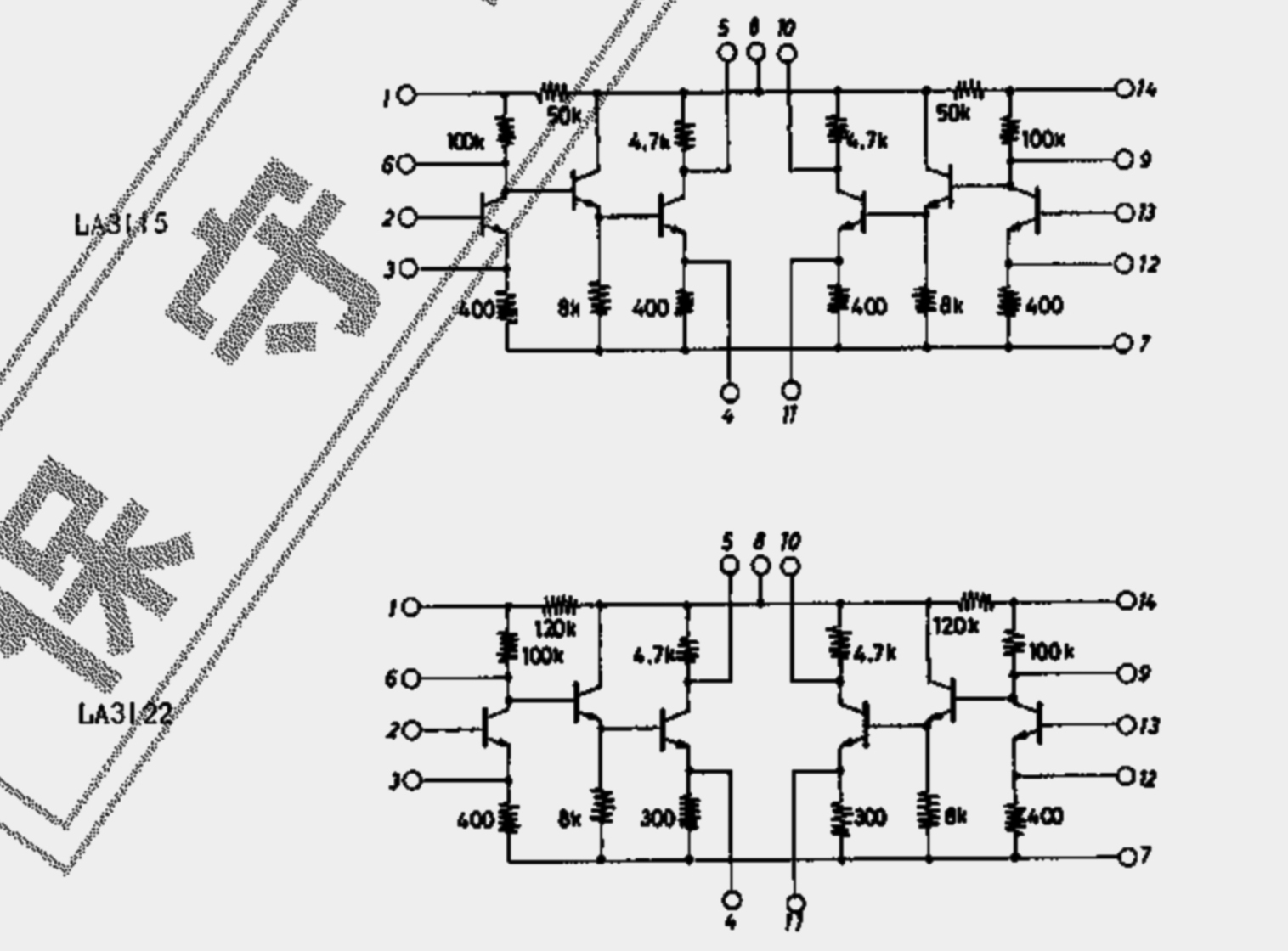
With reference to the LA3122, the voltage gain in Open Loop Gain configuration can be approximated to: Av ~ {(220/0.4)*(4.7/0.3)} or around 8600. This figure is likely to be subject to some considerable error, for one reason, there will later be some internal negative feedback in the form of current-shunt from pin 4 to pin 2. And another, no consideration was made of the base input resistances of each transistor.

A more analytical approach at audio frequencies would suggest that the gain will be of the magnitude: Av ~ [{(220*hie)/(220+hie)}*1/0.4] ✕ [(4.7*hie)/(4.7+hie)*1/0.3]. Here two-ported h-parameter hie is the transistor's input resistance under biased conditions, and can vary from 20Kโ„ฆ to 300Kโ„ฆ (may be less and more?) depending on the type of the transistor. Stage 1 is a very high gain stage, and typically hie ~ 100Kโ„ฆ ... 300Kโ„ฆ, stage2 is just an emitter-follower buffer, and at stage 3, we can expect hie ~ 20Kโ„ฆ ... 100Kโ„ฆ. Setting hie1 ~ 300Kโ„ฆ and hie2 ~ 100Kโ„ฆ, we arrive at an approximation of 4700; much less than 8600, and possibly more realistic? Such an amplifier is gain variable, and its bandwidth will be very restricted.

Applied negative feedback effectively desensitizes any amplifier, and in this case the current-shunt mentioned above, also concurrently applies bias to the base of the first transistor.

Whatever the default gain is, this becomes almost irrelevant. Given that amplifier voltage gain is very high and potentially variable, applying external negative feedback will finally determine the amplifier's overall voltage gain, broaden its bandwidth considerably, and offer excellent voltage gain stability. Apply external negative feedback and we have a closed loop system.


Closed Loop Gain

With the implementation of external voltage-series feedback, Rf (or Zf if it contains reactive elements) active in circuit, the gain can be shown to be Av/(1+Av*๐›ƒ).

And if
Av*๐›ƒ ≫ 1 (which is often desired), then the Closed Loop Gain will gravitate towards A ~ 1/๐›ƒ. At this point, voltage gain is almost independent of open loop gain Av.

The 'beta' term ๐›ƒ is defined as the feedback ratio, which in voltage-series feedback topology is ๐›ƒ=Vf/Vo.

In the particular circuit above we have -

๐›ƒ = Vf/Vo = 400/(400+Zf).

(This ratio is derived from potential divider action)

Simply connecting an impedance Zf (or resistance Rf) between pin 5 and pin 3 will result in a voltage gain of 

A = 1/๐›ƒ
or

A = (400+Zf)/400

Sanyo's LA3122 Circuit Diagram:
Sanyo recommend 220kโ„ฆ for first stage biasing,
and is also part of internal current-shunt feedback.
Zf is the feedback impedance.


Finally, Sanyo state a maximum gain of 40dB in their datasheet example above at 1,000Hz. This can be verified both experimentally, and from 1/๐›ƒ or (400+39000)/400 ~ 98.5.


That is, in decibel form ...

20*LOG(98.5) = 20*1.99 ~ 40dB.


This article is subject to possible changes and corrections.
09/11/2023.


cassettedeckman@gmail.com


Thursday, 14 September 2023

Trio-Kenwood KA-6100 Intergrated Amplifier

 Trio/Kenwood KA-6100

Intergrated Amplifier


Another new purchase.


If any work on this amplifier is pending, then I'll write about it here.

Saturday, 9 September 2023

AKAI AM-2400

The AKAI AM-2400
Integrated Amplifier

Another ebay purchase at a good price.

All that was required was to dry-brush and vacuum-clean the inside of the amplifier, contact-clean the switches, apply lubrication to the switch action, and carefully wash the fascia, controls, and 'work the buttons' with diluted metal polish.

Apart from a few scratches, it's looking good.


Tone Control Board

I've replaced all the capacitors on the tone board; there were (and still are) electrolytic capacitors valued at 0.15uF and 0.22uF that don't need to be electrolytic. The said board was also re-transistorized; replacing the 2SC1213 NPN types with Motorola BC549B types. I am not advising anyone reading this to do the same, although (probably) the 2SC1845/KSC1845 would be a better solution, as the pins are configured in a similar (but reversed) way as the originals. My choice was purely based on my large stock of BC549Bs, and since I wanted to lower my stock in numbers, that's what I did.

I replaced these 2SC1213 transistors in the hope that low level background tone amplifier transistor and general thermal noise could be reduced - you can hear it with headphones when the volume potentiometer has been turned fully anti-clockwise. Later, I hope to replace all carbon resistors within the said board with metal film types. Hopefully this will reduce tone control amplifier noise?

The reader may get the impression that this amplifier is 'noisy', the truth is - it is not. The reason I can hear the thermal or Johnson Noise when the volume potentiometer is turned fully anti-clockwise is that the volume control sits before this audio stage! This means that the push-pull Class A-B power amplifier is receiving the full output of the tone board all the time, and that includes any natural thermal noise.

The only difference the current transistor replacements made are - noise is balanced between left and right, where previously it was more leaning towards the right side. Subjectively, the noise may indeed be lower?, but it's difficult to confirm absolutely.

Below we see the original service manual schematic highlighting the 2SC1222 series as the main audio transistors.

The tone amplifier employs a mixture of Current-Shunt,
and a switchable Voltage-Series feedback topography.

Original 2SC1213 transistors on the tone control board


Note - the alignment of the BC549B on the tone board.


Note - the necessary alignment of the BC549B on the tone board.

Tone Control Board Alterations: (22/09/2022)

Sometime later, there were random 'noise bursts' in the left channel at a very low level, almost imperceptible, but nevertheless they persisted. Later I discovered the apparent source - a dirty contact within the main volume potentiometer VR2, and after cleaning this (again), the problem disappeared. 

Just prior to this work I decided to exchange the BC549B transistors for Fairchild's KSC1845FTA, and KSC1815-GR on this board.

Now we have: TR1=KSC1845,  and TR2=KSC1815

Also of note, the main audio board which serves the power amplifier and voltage regulation has been re-populated with new electrolytic capacitors.

23/09/2023.  This page may be updated if anything relevant to the working, or modifications to the AKAI AM-2400 are undertaken.


Friday, 1 September 2023

Kenwood KT-7500 Tuner

 The Kenwood KT-7500
Stereo FM/AM Tuner


I recently bought this to add to my interest in HiFi receivers and tuners.

The Kenwood KT-7500 is a beautifully engineered and finished piece of HiFi with a gorgeous fascia and controls, and of course high-end performance to match.

This particular version of the KT-7500 is slightly unusual in that there are two switchable de-emphasis configurations to choose from: 25ยตs and 75ยตs time constants; symbolically represented by ๐›•. If a tuner is going to give you a choice, then I would have expected both 50ยตs and 75ยตs time constants, not 25ยตs and 75ยตs!?

The time constant parameter ๐›•, is an accepted convention when describing 'corner frequencies' in the playback of a first-order, low-pass filter frequency response. Each time constant ๐›• is directly linked to a corner frequency fc.

Here in the UK, the playback de-emphasis curve adheres to a time constant of 50ยตs, that is ๐›• = 50/1000000 seconds, whereas, in the United States and Canada, they employ the 75ยตs time constant.

Therefore, it is quite possible that this KT-7500 was purchased in the US or Canada back in the late 1970s? I say this since 25
ยตs was intended to be used for Dolby encoded broadcasts in the United States, possibly Canada too? For this to work correctly, a Dolby outboard would be required?

An explanation of de-emphasis, and the associated time constant will be explained at, or near the end of this article.

The KT-7500 in its Wooden Housing:


Opening up the KT-7500 reveals a beautifully laid out circuit.


Highlighted above in white is the final low-pass de-emphasis circuit that needs to be modified so that both 50
ยตs and 75ยตs time constants are easily accessed, at present I've only 25ยตs (for a Dolby outboard?) or 75ยตs (United States) to choose from.

Observe below, a picture taken for the original advert by the seller, and the limited choice: 75ยตs (US or Canada) or 25ยตs (Dolby encoding) de-emphasis setting.


Identifying De-emphasis Stages

Studying the schematic for the KT-7500, we are able to track down the output stages, and identify the de-emphasis low-pass circuit.


Both left and right channels have been highlighted for convenience: right in red, and left in blue.

Studying the circuit diagram reveals that a NJM4558 dual OP Amp has been used in the final stages of audio post-processing; that is FM de-emphasis.

The OP Amp appears to be configured in a non-inverting, first-order low-pass state. Similar to that shown below -


The derivation for the voltage gain for this non-inverting amplifier can be shown to be: 

 Av(ฯ‰) = 1 + Zf(ฯ‰)/R

Where Zf(ฯ‰) is the impedance of the parallel network containing the 33kโ„ฆ resistor and the 750pF (and, or the 1500pF) capacitance. The R is the 2kโ„ฆ resistance as shown above.

This voltage amplifier's gain is frequency dependent, but can easily act as a voltage follower if Zf→0โ„ฆ; in that case the gain is simply unity, ie 1.

However, returning to our low pass de-emphasis amplifier and filter - in terms of the resistive and capacitive components, the complex form of the voltage gain of the OP Amp in this non-inverting arrangement is:


Where Rf = 33000โ„ฆ, C = 750pF or 2250pF, and R1 = 2kโ„ฆ.

Note: In the KT-7500, C is actually switchable between 750pF and (750+1500)pF. 

Also, be mindful that periodic frequency f (Hz) is related to angular frequency ฯ‰=2๐ฟf (radians/second), or f=2๐ฟ/ฯ‰.

In the above 'complex' form, both voltage gain and input vs output phase shift can be analyzed.

In an attempt to keep this write up as simple as possible, the mathematical issues of derivation of formulae are going to be by-passed.

Computing OP AMP Gain Av(f) vs Frequency (Hz)

Applying a complex conjugate operator to the above expression, and we have ...


And so, the modulus or absolute value of the gain is ...


Mapped out, it will look like this ...

Frequency Response Curves
for CR value of: C x R = 50ยตs


If my calculations are correct, the plot in red would be the theoretical curve if the OP Amp was in an inverting configuration, and in blue is the theoretical plot for our non-inverting KT-7500.


Corner Frequency and Time Constant

The corner frequency is that frequency f, for which 

2๐ฟfCR = 1, 

or

f = 1/{2๐ฟCR} Hz.  

The gain then becomes .....


Under these conditions, and without the '1' term, the gain is (Rf/R1)×(1/√2)⁢ or -3dB below its maximum value. However, because the gain for this OP Amp configuraton is Av = 1 + Zf/R, the '1' offsets this calculation a little.

The time constant ๐›• mentioned earlier is generally derived from RC networks and their ability to charge or discharge, and in particular - the initial rate at which charging/discharging occurs on response to a voltage step function.

๐›• definition: If this initial rate of charge were to be maintained, then the time taken for the capacitor to become fully charged or discharged is equal to: C x R seconds.

That is ...

๐›•=CR

The reader may have already deduced that frequency f and ๐›• are related, that is, at the corner frequency fc: fc = 1/{2๐ฟ๐›•}.

UK FM De-emphasis

Here in the UK, the 50ยตs de-emphasis time constant
๐›• is employed, it is directly related to a de-emphasis corner frequency.

fc = 1/{2๐ฟแง50ยตs} = 1000000/{2๐ฟแง50} = 3183Hz.

In the context of the KT-7500, and to obtain ๐›•=50ยตs, C needs to be 1500pF, neglecting component tolerances, the actual values of CR used above gives ...

 ๐›•=1500pF*33Kโ„ฆ = 49.5ยตs

or 

fc = 1000000/{2๐ฟแง49.5} = 3215Hz.

Now examine the above plot to confirm the -3dB drop at approximately 3183Hz. This equates to (1/√2)*17.5 at 3183Hz.

United States/Canadian De-emphasis

In the US and Canada,
๐›•=75ยตs, that is ...

fc = 1000000/{2๐ฟแง75} = 2122Hz.


Turning our attention to the Kenwood KT-7500, the slide switch is turned to '75us' and so we obtain C=(750pF+1500pF)=2250pF, which leads to 
๐›•=2250pF*33Kโ„ฆ = 74.25ยตs. Which in practical terms yields: fc = 2143Hz. Again, we neglect small variations in component values.

Concerning Dolby de-coding de-emphasis, it is left to the reader to compute fc from
๐›•=25ยตs.

Re-configuring the Kenwood KT-7500 De-emphasis

Returning to the problem of incorrect de-emphasis for this KT-7500, and inspecting the values of the polystyrene (close tolerance) capacitors suggests that swapping both sets of capacitors will provide the correct playback equalization that I require.


Note: JRC4558 dual OP Amp used in this Kenwood.


Previously, playback from FM transmissions sounded as if the treble control had been turned down by a few dB. All good now!

14/09/2023: This article may be subject to minor corrections, and additions.