Modelling
of the 1970s
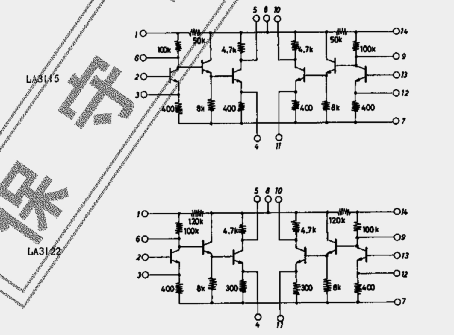
TA7122/ECG1085
Three
Stage Voltage Amplifier

Actual circuit is to the right of Vin.
Left hand side represents a signal generator.
The
Toshiba TP7122 (and ECG1085?) voltage amplifier was commonly used by Sony and
others in their cassette decks and reel to reel machines of the
1970s. It was likely used in many other
applications. It also resembles Sanyo’s own LA3122.
The TA7122AP or ECG1085 may indeed be difficult to source today, which is why I decided to investigate building an equivalent, effective configurable voltage amplifier.
The
above amplifier comprises of three stages:
- Stage 1 T1 – a high gain voltage amplifier,
- Stage 2 T2 – a buffer, unity gain emitter-follower, and finally
- Stage 3 T3 – a final high gain (but less then Stage 1) voltage amplifier.
The pins as labelled by ECG Semiconductors form part of the powering, and user defined network and feedback system.
Current Shunt feedback from pins 5 to pin 2 help stabilize the amplifier’s gain. Additionally, both T1 and T3 circuits are also configured in current-series feedback topologies. The feedback values of Re in both T1 and T3 stages are small, although I suspect all three Re resistances in each of the emitters are mainly employed to prevent thermal runaway?
To further stabilise the amplifier and thus set a usable gain and bandwidth, voltage-series feedback network from pin 6 to pin 3 is required; marked in blue.
Analysis
Circuit analysis can often be difficult, and so the model offered here is slightly compromised. That is – it is assumed that the operation of this amplifier is restricted to audio frequencies, and no analysis has been made regarding the effects of parasitic capacitances and inductances, resulting in possible, but unlikely self oscillation. Often we see small ceramic capacitors of several pF placed strategically to avoid full phase inversion feeding back to the input – hence self oscillation.
Stage1
T1: Very High Gain Voltage Amplification

|
Simplified Hybrid Parameter Equivalent |

Considering the effects of hie, and on the application of Kirchoff's voltage and current laws we arrive at the following Vo vs Vin model -

or alternatively, if the effects of ri and Re1 are ignored (in the left side of the denominator) a simplified model will be ...

In
a low loaded state, we can expect the gain to be very high.
(a)
ro = 20KΩ
Av
= 820*20/(820+20)*(1/0.22) = 88
(b)
ro = 300KΩ
Av
= 820*300/(820+300)*(1/0.22) = 998
I expect the first stage transistor to be a sensitive high current gain (high hfe) type, similar to that of the modern and popular KSC1845-FTA. With such a dramatically variable voltage gain, there will be consequences – the main being saturation and bandwidth. However, more negative feedback will desensitise the amplifier to a more stable manageable system as we will see later.
For any amplifier there is always a gain × bandwidth constant. Since the gain was anticipated to be so high at this stage, clearly the bandwidth was going to be severely compromised. Even at just 500Hz, the gain of this single stage was dropping, so it was decided to set the testing at 50Hz and under, where gain was close to its maximum.
Observing traces on a 10MΩ-configured-input oscilloscope as accurately as possible, I arbitrarily set the input and got: VRL1=-1.45v, and Vin=2.75mV (not VS), the computed gain was -
Av
= -1.45v/0.00275
= -527
ro=50KΩ, Av ~ 205
ro=100KΩ, Av ~ 375
ro=150KΩ, Av ~ 517
ro=200KΩ, Av ~ 638
Then under these biasing conditions, ro (1/hoe) was estimated at around 150kΩ.
Stages
1,2,3: Full Circuit Without External Feedback Network

This time, Vs is measured in an open-circuit state to avoid internal resistances (RS ~600Ω) interfering with the results. Again, using the oscilloscope visually to compute AV,
VS
= 7.4mV, and VRE3
= 20.8v
(peak-to-peak measurements on both accounts)
gives
Av
= 2810
(The expression above was derived by modelling the circuit where RE1=0. Modelling with RE1 >0 is more complex, I may later write an article on how both were derived!)
Of interest, RE1 was later short-circuited, and so the small amount of feedback offered by RE1 was theoretically zeroed, here the gain was examined: VS = 7.2mV, and VRE3 = 22v, and so
Av
= 3056
RE1=0.22KΩ, error = |3833-2810|/3833 ~ 26.7%
RE1=0Ω,
error = |3833-3056|/3833 ~ 20.3%.
So,
as a stand-alone amplifier, in this present form we can expect a
large gain of somewhere between 2500 and 4000, but still with a restricted bandwidth. However, further negative
feedback will desensitise the amplifier,
and impresses gain and bandwidth stability.
Full Circuit with Final Feedback Network β
According
to feedback theory,
AVCL
= AOL/(1+AOL·β),
(AVCL: closed loop gain, AOL :open loop gain)
and if
AOL·β>>1
then
AVCL ~ 1/β,
where
β
is a feedback ratio (β≡VE1/Vo) and can be shown via potential divider action to be
β =
RE1/(RF2+RE1)
Applying
this to the T1/T2/T3
full circuit -
To
drive the amplifier into a stable amplification environment, and
much
broader bandwidth, we can arbitrarily
set RF2
= 10KΩ,
and with RE1=0.22KΩ,
AVCL=
(10+0.22)/0.22
= 46.5
Comparing
this
to
actual measurement, VO
= 4v (p2p)
with
VS
= 91.6mV (p2p), we have -
AVCL
=
4/0.0916 = 43.7
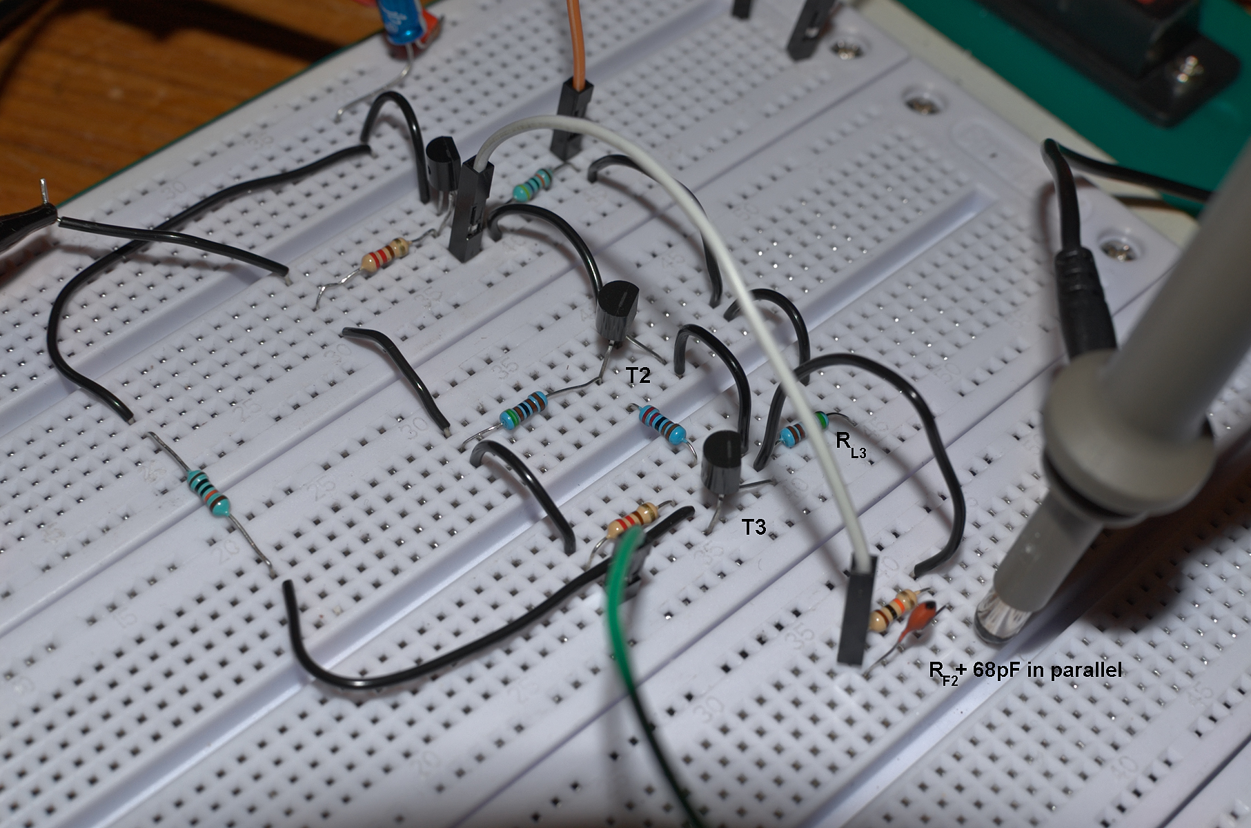
Square Wave Response
As a quick indication of the amplifier's stability, the input was subjected square wave excitation at both 1Khz, and 10Khz with a 10KΩ load across Vo.
Recalling amplifier expression AOL/(1+AOL·β) again, a rise in output can be attributed to the denominator exhibiting some pronounced phase shifting at high frequencies. The gradual but apparent higher frequency phase shifting suggests that the term |1+AOL·β| is behaving as |1-AOL·β|, and thus lowering its value to increase overall gain. Should this amplifier have become very unstable (very unlikely), then we'd presume that the denominator term move closer to zero, ie |1-AOL·β| → 0.
Shown below are traces of two square wave input signals - both at 10Khz. Note the small overshoot on the first, and then compare to the next when a compensating capacitor Cf is added.

On excitation of 10Khz input.
Observe a small amount of overshoot; the amplifier is relatively stable.
With the addition of a compensating 68pF ceramic capacitor across RL2 (Cf), the amplifier is further stabilised, or dampened. This inclusion of Cf is very effective as this revised feedback attenuates the 'lift' around 100Khz-200Khz.

| |
Very stable amplification, |

In the present setup, the amplifier with a Avcl gain of approximately 44, is delivering a -3dB-0dB-3dB bandwidth which is slightly better than 5Hz - 200Khz.
Amplifier Input and Output Impedance
Amplifier Distortion
Not yet measured.
*This article is subject to corrections and additions without notice. 18/11/2023
cassettedeckman@gmail.com